- 您现在的位置:买卖IC网 > Sheet目录1917 > DSPIC30F4011-30I/ML (Microchip Technology)IC DSPIC MCU/DSP 48K 44QFN
2010 Microchip Technology Inc.
DS70135G-page 147
dsPIC30F4011/4012
20.9
Module Power-Down Modes
The module has 3 internal power modes. When the
ADON bit is ‘1’, the module is in Active mode; it is fully
powered and functional. When ADON is ‘0’, the module
is in Off mode. The digital and analog portions of the
circuit are disabled for maximum current savings. In
order to return to the Active mode from Off mode, the
user must wait for the ADC circuitry to stabilize.
20.10 A/D Operation During CPU Sleep
and Idle Modes
20.10.1
A/D OPERATION DURING CPU
SLEEP MODE
When the device enters Sleep mode, all clock sources
to the module are shut down and stay at logic ‘0’.
If Sleep occurs in the middle of a conversion, the
conversion is aborted. The converter will not continue
with a partially completed conversion on exit from
Sleep mode.
Register contents are not affected by the device
entering or leaving Sleep mode.
The ADC module can operate during Sleep mode if the
A/D clock source is set to RC (ADRC = 1). When the
RC clock source is selected, the ADC module waits
one instruction cycle before starting the conversion.
This allows the SLEEP instruction to be executed,
which eliminates all digital switching noise from the
conversion. When the conversion is complete, the
DONE bit is set and the result is loaded into the
ADCBUFx register.
If the A/D interrupt is enabled, the device wakes up
from Sleep. If the A/D interrupt is not enabled, the ADC
module is then turned off, although the ADON bit
remains set.
20.10.2
A/D OPERATION DURING CPU IDLE
MODE
The ADSIDL bit selects if the module stops on Idle or
continues on Idle. If ADSIDL = 0, the module continues
operation on assertion of Idle mode. If ADSIDL = 1, the
module stops on Idle.
20.11 Effects of a Reset
A device Reset forces all registers to their Reset state.
This forces the ADC module to be turned off, and any
conversion and acquisition sequence is aborted. The
values that are in the ADCBUFx registers are not
modified. The A/D Result register contains unknown
data after a Power-on Reset.
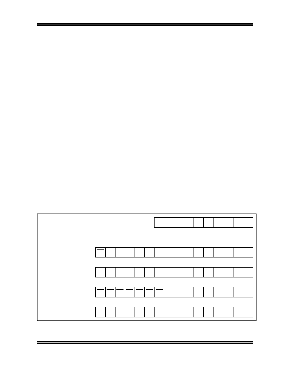
20.12 Output Formats
The A/D result is 10 bits wide. The data buffer RAM is
also 10 bits wide. The 10-bit data can be read in one of
four different formats. The FORM<1:0> bits select the
format. Each of the output formats translates to a 16-bit
result on the data bus.
Write data will always be in right justified (integer)
format.
FIGURE 20-4:
A/D OUTPUT DATA FORMATS
RAM Contents:
d09 d08 d07 d06 d05 d04 d03 d02 d01 d00
Read to Bus:
Signed Fractional (1.15)
d09 d08 d07 d06 d05 d04 d03 d02 d01 d00
000000
Fractional (1.15)
d09 d08 d07 d06 d05 d04 d03 d02 d01 d00
000000
Signed Integer
d09 d09 d09 d09 d09 d09 d09 d08 d07 d06 d05 d04 d03 d02 d01 d00
Integer
0
d09 d08 d07 d06 d05 d04 d03 d02 d01 d00
发布紧急采购,3分钟左右您将得到回复。
相关PDF资料
DSPIC30F4013-30I/ML
IC DSPIC MCU/DSP 48K 44QFN
DSPIC30F5013-30I/PT
IC DSPIC MCU/DSP 66K 80TQFP
DSPIC30F5015-30I/PT
IC DSPIC MCU/DSP 66K 64TQFP
DSPIC30F6010-20E/PF
IC DSPIC MCU/DSP 144K 80TQFP
DSPIC30F6010A-30I/PF
IC DSPIC MCU/DSP 144K 80TQFP
DSPIC30F6013A-30I/PF
IC DSPIC MCU/DSP 132K 80TQFP
DSPIC30F6014-30I/PF
IC DSPIC MCU/DSP 144K 80TQFP
DSPIC33EP512MU814-I/PL
IC DSC 16BIT 512KB 144LQFP
相关代理商/技术参数
DSPIC30F4011-30I/P
功能描述:数字信号处理器和控制器 - DSP, DSC 16bit Signal Cntrlr RoHS:否 制造商:Microchip Technology 核心:dsPIC 数据总线宽度:16 bit 程序存储器大小:16 KB 数据 RAM 大小:2 KB 最大时钟频率:40 MHz 可编程输入/输出端数量:35 定时器数量:3 设备每秒兆指令数:50 MIPs 工作电源电压:3.3 V 最大工作温度:+ 85 C 封装 / 箱体:TQFP-44 安装风格:SMD/SMT
DSPIC30F4011-30I/PT
功能描述:数字信号处理器和控制器 - DSP, DSC 16 Bit MCU/DSP 30M 48KB FL RoHS:否 制造商:Microchip Technology 核心:dsPIC 数据总线宽度:16 bit 程序存储器大小:16 KB 数据 RAM 大小:2 KB 最大时钟频率:40 MHz 可编程输入/输出端数量:35 定时器数量:3 设备每秒兆指令数:50 MIPs 工作电源电压:3.3 V 最大工作温度:+ 85 C 封装 / 箱体:TQFP-44 安装风格:SMD/SMT
DSPIC30F4011T-20E/ML
功能描述:数字信号处理器和控制器 - DSP, DSC 16 Bit MCU/DSP 44LD 20M 48KB FL RoHS:否 制造商:Microchip Technology 核心:dsPIC 数据总线宽度:16 bit 程序存储器大小:16 KB 数据 RAM 大小:2 KB 最大时钟频率:40 MHz 可编程输入/输出端数量:35 定时器数量:3 设备每秒兆指令数:50 MIPs 工作电源电压:3.3 V 最大工作温度:+ 85 C 封装 / 箱体:TQFP-44 安装风格:SMD/SMT
DSPIC30F4011T-20E/PT
功能描述:数字信号处理器和控制器 - DSP, DSC 16 Bit MCU/DSP 20M 48KB FL RoHS:否 制造商:Microchip Technology 核心:dsPIC 数据总线宽度:16 bit 程序存储器大小:16 KB 数据 RAM 大小:2 KB 最大时钟频率:40 MHz 可编程输入/输出端数量:35 定时器数量:3 设备每秒兆指令数:50 MIPs 工作电源电压:3.3 V 最大工作温度:+ 85 C 封装 / 箱体:TQFP-44 安装风格:SMD/SMT
DSPIC30F4011T-20I/ML
功能描述:数字信号处理器和控制器 - DSP, DSC DIG SIG CONTR RoHS:否 制造商:Microchip Technology 核心:dsPIC 数据总线宽度:16 bit 程序存储器大小:16 KB 数据 RAM 大小:2 KB 最大时钟频率:40 MHz 可编程输入/输出端数量:35 定时器数量:3 设备每秒兆指令数:50 MIPs 工作电源电压:3.3 V 最大工作温度:+ 85 C 封装 / 箱体:TQFP-44 安装风格:SMD/SMT
DSPIC30F4011T-20I/PT
功能描述:数字信号处理器和控制器 - DSP, DSC 16 Bit MCU/DSP 20M 48KB FL RoHS:否 制造商:Microchip Technology 核心:dsPIC 数据总线宽度:16 bit 程序存储器大小:16 KB 数据 RAM 大小:2 KB 最大时钟频率:40 MHz 可编程输入/输出端数量:35 定时器数量:3 设备每秒兆指令数:50 MIPs 工作电源电压:3.3 V 最大工作温度:+ 85 C 封装 / 箱体:TQFP-44 安装风格:SMD/SMT
DSPIC30F4011T-30I/ML
功能描述:数字信号处理器和控制器 - DSP, DSC 16 Bit MCU/DSP 44LD 30M 48KB FL RoHS:否 制造商:Microchip Technology 核心:dsPIC 数据总线宽度:16 bit 程序存储器大小:16 KB 数据 RAM 大小:2 KB 最大时钟频率:40 MHz 可编程输入/输出端数量:35 定时器数量:3 设备每秒兆指令数:50 MIPs 工作电源电压:3.3 V 最大工作温度:+ 85 C 封装 / 箱体:TQFP-44 安装风格:SMD/SMT
DSPIC30F4011T-30I/PT
功能描述:数字信号处理器和控制器 - DSP, DSC 16 Bit MCU/DSP 30M 48KB FL RoHS:否 制造商:Microchip Technology 核心:dsPIC 数据总线宽度:16 bit 程序存储器大小:16 KB 数据 RAM 大小:2 KB 最大时钟频率:40 MHz 可编程输入/输出端数量:35 定时器数量:3 设备每秒兆指令数:50 MIPs 工作电源电压:3.3 V 最大工作温度:+ 85 C 封装 / 箱体:TQFP-44 安装风格:SMD/SMT